
Blog
Anti-Static PEEK Profiles: Beyond “Anti-Static”—Engineered for Exceptional Performance

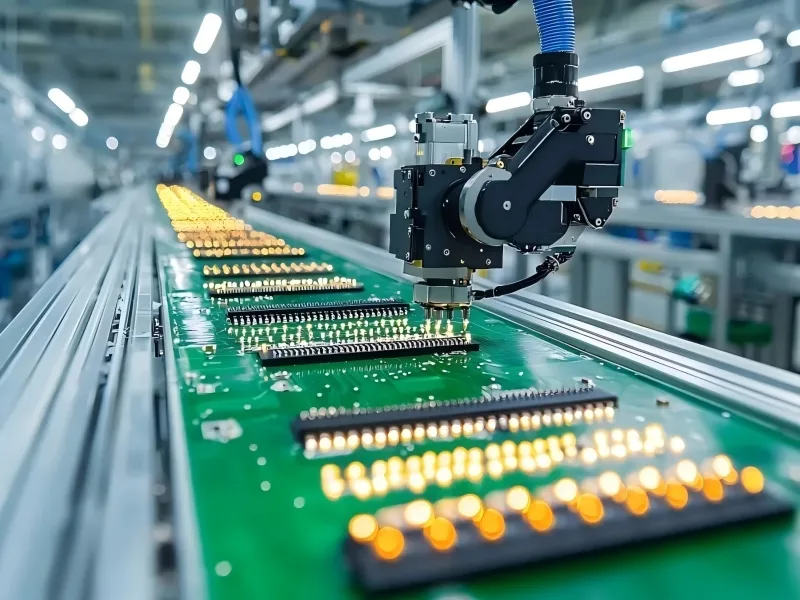
As semiconductor manufacturing processes continue to evolve and advanced packaging technologies rapidly progress, industry requirements for material performance are reaching new heights. Beyond basic functional capabilities, factors such as dimensional stability, cleanliness, anti-static reliability, and machining consistency have become critical to ensuring the stable operation of production lines.
Electrostatic discharge (ESD) can lead to component damage, dust adsorption, and yield fluctuations. Consequently, engineering plastics with stable anti-static properties are systematically becoming a premier material choice for semiconductor manufacturing and testing phases.
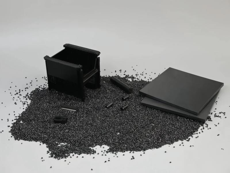
Developed specifically to meet these demanding application requirements, our anti-static PEEK profiles strike a perfect balance between ESD protection, mechanical properties, and processing stability. They are ideally suited for semiconductor, electrical, and electronic applications that demand exceptional comprehensive material performance.
Stable ESD Performance Tailored for Diverse Semiconductor Applications
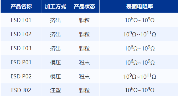
Surface resistivity is the core metric for evaluating anti-static effectiveness. Our PEEK profiles strictly control this indicator within the customer-specified range.
- Specification Sheet: 106Ω∼109Ω
- Actual Measured Range: Consistently stable between 106Ω∼108Ω with highly uniform resistance.
This exceptional uniformity effectively prevents static accumulation and sudden discharges in ESD-sensitive stages—such as wafer transport and chip testing—safeguarding the production environment and product yield right from the source.
Furthermore, we utilize a specialized “Solution – Grinding – High-Speed” dispersion process, which has already been field-proven in high-end products like PEEK wafer carriers:
- Solution Dispersion: Enhances the surface activity of the PEEK matrix.
- Grinding Dispersion: Ensures the conductive additives bond tightly and seamlessly with the base material.
- High-Speed Dispersion: Reaches a homogeneous fusion of all components.
Thanks to this advanced process, the internal resistance uniformity of our PEEK profiles far outperforms standard anti-static PEEK, successfully eliminating localized resistance fluctuations, weak points, or batch-to-batch variations caused by conductive agent agglomeration.
Balanced Mechanical Strength and Machining Excellence
High strength and high modulus provide these profiles with dependable structural support and superior machining characteristics.
Standard anti-static sheets often suffer from burrs and rough edges after CNC machining. Additionally, when put into service, a lack of sufficient strength and modulus can cause structural failure, leading to the sagging and deformation of test fixtures.
In contrast, parts machined from PEEK ESD E03 profiles feature excellent structural integrity, pristine edges, and burr-free machining. This is made possible by the material’s superior baseline strength and modulus—providing enough rigidity to resist deformation and the “drawing effect” caused by cutting tools. Moreover, enhanced structural support extends the service life of the components, reducing downtime and maintenance costs caused by frequent fixture replacements on the production line.
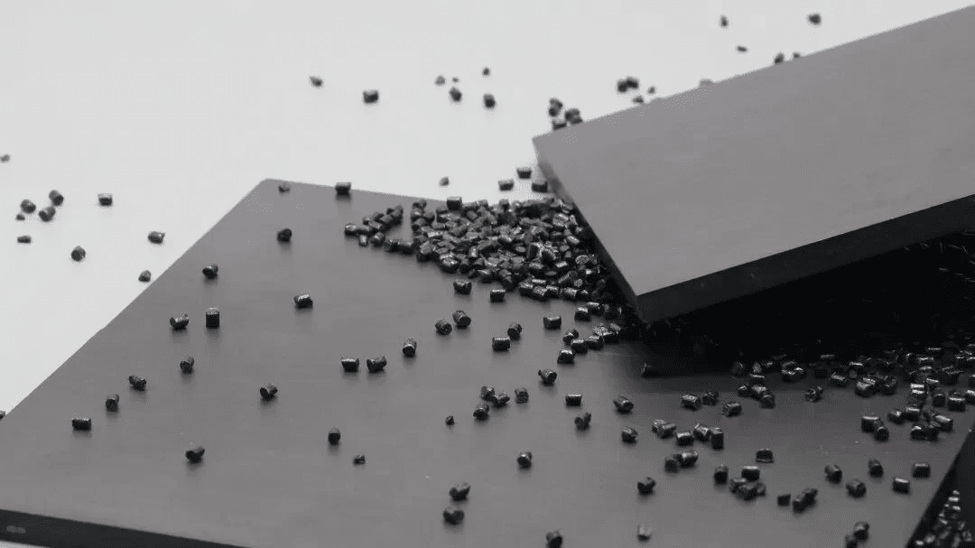
Low Warpage and High Dimensional Stability Meet Precision Machining Demands
For precision components such as semiconductor test fixtures and high-temperature matrix trays, material dimensional stability during machining and end-use is paramount. In highly automated production lines where wafer sizes are fixed, even a minor dimensional deviation in the teeth of a wafer carrier can cause catastrophic wafer damage. Furthermore, these parts must maintain their structural integrity through rigorous high-low temperature cycles.
Based on internal testing, PEEK ESD E03 profiles exhibit remarkably low warpage in specific sample dimensions. For instance, testing on a ring sample with a thickness of 29 mm and an outer diameter of 158 mm yielded the following results:
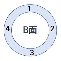
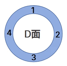
Backed by precise formulation optimization, mature molding technology, and strict post-molding stress-relief treatments, our PEEK sheets fully satisfy the precision machining requirements of components across various dimensions.
Fundamentally, warpage reflects the uniformity of internal stress within a material. The low warpage achieved by our PEEK profiles stems from comprehensive, full-chain process control—spanning from precise extrusion temperature regulation to optimized annealing processes. This targets and minimizes internal stress, eliminating the common risk of warpage and deformation found in standard anti-static sheets.
Full-Condition Adaptability: High Temperature, Wear, and Chemical Resistance
Semiconductor manufacturing environments are frequently plagued by high temperatures, corrosive media, and constant mechanical friction. ZYPEEK anti-static profiles deliver outstanding performance under these harsh conditions:
- High-Temperature Resistance: Features a long-term continuous working temperature of up to 260°C, with the ability to withstand even higher temperatures short-term. Mechanical properties remain stable at elevated temperatures, making it ideal for demanding environments like high-temperature matrix trays and burn-in test sockets.
- Wear Resistance: Balanced surface hardness and lubricity ensure that the material will not scratch silicon wafers or chips during direct contact. It minimizes particle generation during machining or operation, making it highly compatible with cleanroom environments.
- Chemical Resistance: Aside from concentrated sulfuric acid, it exhibits robust resistance to acids, bases, salts, and various organic solvents. It remains stable when exposed to the diverse corrosive media used in semiconductor manufacturing, significantly extending product lifespan.
- Low Metal Ion Elution: In high-temperature, high-friction environments, residual metal ions remain far below industry thresholds, effectively protecting wafer yield even under thermal stress.
Why Choose ZLPEEK? Three Core Capabilities to Realize Your Material Solutions
While product performance is vital, the foundational questions during engineering plastic selection center on sustainable delivery, rapid customization based on customer needs, and minimizing validation costs.
1. Advanced Material Modification & Formulation R&D
Leveraging years of specialized experience in PEEK material research and development, our company continuously advances material innovations in conductivity, reinforcement, wear resistance, and self-lubrication. We offer targeted formulation optimizations tailored to diverse application requirements.
2. High-Efficiency Response Speed
Upon receiving customer feedback or new specifications, we provide optimized solutions within one week and deliver physical samples within half a month. Relying on our in-house modification and profile extrusion production lines, we achieve rapid synergy from formula adjustment to sample preparation, significantly accelerating your project development and validation cycles.
3. Application Verification & Machining Support
While standard material suppliers often provide only raw materials and physical property datasheets—leaving subsequent application verification entirely to the customer
Utilizing our own profile extrusion and machining capabilities, we conduct pre-evaluations of new grades or optimized formulas during the development phase. We perform verification testing against typical application scenarios, including wafer transport, high-temperature environment endurance, and machining compatibility.
Through this early-stage application verification, customers receive more than just basic physical data—they gain reference test results mapped to actual working conditions, boosting material adoption efficiency and shortening verification cycles. Furthermore, our internal machining and sample development capabilities allow us to directly machine and validate specific dimensions of fixtures, rings, and strips. We conduct internal testing on machining performance and dimensional stability to provide clear, direct technical references for your project development.
Consistency is reflected not only in the material data itself, but also in product uniformity, processing stability, and long-term field performance. Built around the rigorous application needs of the semiconductor and related industries, our anti-static PEEK profiles continually optimize material performance and process control to provide customers with a more stable, reliable material solution.